1. Blog>
  2. Generate Gerber file from Kicad

Generate Gerber file from Kicad

by: Jul 03,2017 77494 Views 21 Comments Posted in Help Center

Gerber Kicad PCB design Tutorial

Now you can place order directly by PCBWay Plugin for KiCad


Usually, it is easier to generate Gerber files using Kicad than other PCB design software. All you need to do is to select the necessary layers and to not forget generating the DRILL file. Now, let’s get started!

1. Open your .kicad_pcb file

After opening your Kicad project - .pro file, you can double click the .kicad_pcb file or click the “PCBNew” button to open your PCB editor.

 kicad1.png

2. Plot your Kicad PCB as Gerber files

Click the “File” menu -->”Plot” and choose the necessary layers shown as below (for 2 layer boards), then click the “Plot” button to generate the related layers.

PCBNew plot.png

The necessary layers for 2-layer PCB could be:

Top Layer: pcbname.GTL

Bottom Layer: pcbname.GBL

Solder Mask Top: pcbname.GTS

Solder Mask Bottom: pcbname.GBS

Silk Top: pcbname.GTO

Silk Bottom: pcbname.GBO

Drill Drawing: pcbname.TXT

Board Outline:pcbname.GML/GKO

Note: In order to facilitate our access to your files, please do NOT check the "Include extended attributes" before Plot.

Do NOT check "Use extended X2 format", otherwise, the format will not be accpeted.


3. Generate the drill file

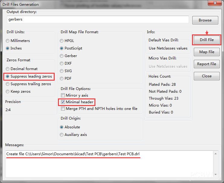
Before closing the plot window, you need also generate the drill for manufacturing. Select “Suppress leading zeros”  and “Minimal header” and click “Drill File” button as following shown.

1.Generate Drill.png

4. Check the Gerber files in GerbView

Now you have finished the job. But you should always check whether your Gerber files are working or not. Open the “GerbView” and check what your board looks like before sending it to manufacturer.

Gerber view.png

Now you can see your board like this.

final.png

5.Compress all the files in a single .zip file


The final step is to Compress all the files in a single .zip file, then you can fill out the form about your PCB parameters ( size, quantity , layers , thickness , etc ) on our “PCB Instant quote” page and upload your .zip ( Gerber ) file to PCBWay online system, our engineers will check it again and feedback to you if any problems happen before it can be fabricated. Here we go!


See "Generate Position File in Kicad"

Check for Kicad 5.1.6

https://www.pcbway.com/blog/help_center/Generate_Position_File_in_Kicad.html

Join us
Wanna be a dedicated PCBWay writer? We definately look forward to having you with us.
  • Comments(21)
Upload photo
You can only upload 5 files in total. Each file cannot exceed 2MB. Supports JPG, JPEG, GIF, PNG, BMP
0 / 10000
  • This tutorial is deprecated. Please delete it or make the new plugin line red. from me who totally followed this and get my file rejected for missing solder mask layer

    PCBWay Team 2023-05-19 16:03:51Reply

    We will update this article based version7.0.Now you can place order directly by PCBWay Plugin for KiCad.For details on how to use it, see the link.https://www.pcbway.com/blog/News/PCBWay_Plug_In_for_KiCad_3ea6219c.html

    PCBWay Team 2023-05-19 17:15:53Reply

    The solder mask is not checked in the picture, we have checked it now.

    Reply
  • The KiCad plot window looks a little bit different now than it did when this was originally posted. Can PCBWay make an updated tutorial? I'm having trouble ordering my boards, and I think it's due to several options that aren't even shown in these photos.

    Engineer 2020-09-18 21:54:36Reply

    +1 for having an updated screenshots from KiCad 5.1

    gary fry 2021-06-06 23:30:19Reply

    +1 to that

    Carl 2021-06-09 10:17:40Reply

    Maybe you can check this one: https://www.pcbway.com/blog/help_center/Generate_Gerber_file_from_Kicad_5_1_6.html

    Reply
  • Edward Peguillan III 2020-08-26 22:00:26Reply

    Thank you for showing the way the window looks in the current version of KiCad. Can you edit your OP and replace the photo with this one? It took me an hour to find a reference for how to setup my geber files for PCBWay ordering.

    PCBWay Support Team 2020-08-27 10:23:31Reply

    Thanks for your advice.

    Reply
  • Are these the correct settings?

    PCBWay Support Team 2020-08-27 09:53:07Reply

    Yes, Edward, it is correct.

    Reply
  • When using a recent version of KiCAD (5.1.4 on Windows) if I check "Exclude PCB edge layer from other layers" as reported above, when I upload gerber file on instant pcb quote dimensions are wrong, if I disable the checkbox, dimensions are reported correctly. It's wrong uncheck that?

    PCBWay Support Team 2019-12-10 16:09:30Reply

    Hello Fabrizio, you might forget to check Edge.Cuts, the default is not selected, it will be fine if selected. (See the below picture.) Regarding of the "Exclude PCB edge layer from other layers", if you do not check, the profile of each layer will appear.

    Reply
  • Is this still the way to go with KiCAD 5? Looks like the drill-file dialog has changed ...

    PCBWay Support Team 2018-08-27 09:24:56Reply

    Yes, you are supposed to choose the options mentioned above and then it will output correctly.

    Richard Pierce 2018-10-17 15:03:50Reply

    Can I submit a job with drill file with the units set to mm instead of inches? Because now in KiCad 5 apparently Gerbview doesn't scale the plot and drill files the same unless the drill file units match the plot units (mm).

    PCBWay Support Team 2018-10-18 09:29:46Reply

    yes, both mm and inches settings are OK

    Reply
  • This is great. Do you know how to generate a pick and place centroid file?

    Reply
  • When using recent version of KiCAD (In my case; "Version: no-vcs-found-4838869~61~ubuntu16.04.1, release build"), in the "Plot" dialog, you must un-check the box which reads; "Include extended (X2) attributes" in order for PCBWay to be able to read the Gerber files.

    Reply
  • Simply works. Nice tutorial.

    Reply
Back to top